ilicon hetero-junction technology (c-Si HJ) consists of thin amorphous silicon layers on mono-crystalline silicon wafers and allows for photovoltaic solar cells with energy conversion efficiencies above 20 %.
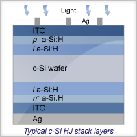
The basic device features on the front (illumination) side successively an intrinsic a-Si:H passivation layer and a p-doped amorphous silicon emitter both deposited by plasma enhanced chemical vapor deposition (PECVD). On top of the silicon layers, an antireflective transparent conductive oxide (TCO) is deposited by physical vapor deposition (PVD) and the charge collection is made by a screen-printed metallic contacting grid. On the back side, the stack is realized of an intrinsic a-Si:H passivation layer, a back-surface field (BSF) layer made of n-type amorphous silicon both deposited by PECVD, a TCO layer and a metallic contacting layer.
hin Film Silicon Solar Cells consist of high efficiency hydrogenated amorphous (a-Si:H) and microcrystalline (µc-Si:H) silicon single-junctions and multi-junctions solar cells in the superstrate configuration (p-i-n).
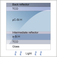
Microcrystalline silicon is of particular interest when combined with amorphous silicon in a solar cell tandem configuration, commonly called "micromorph", as the different optical band gaps of these materials allow for the active conversion of a larger part of the solar spectrum. In such combination, a top a-Si:H cell absorbs light with wavelengths up to 800 nm while the µc-Si:H bottom cell can absorb light in the near infrared region, allowing for larger attainable conversion efficiencies.
Microcrystalline silicon is a complex material that exhibits a wide range of possible microstructures depending on both the deposition conditions and substrate material. Many efforts have been laid in the past years in understanding the growth mechanisms of this material and the relationship between microstructure and solar cell efficiency.