his all-new technology sets a new benchmark in the PECVD deposition universe.
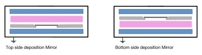
The INDEOtec team has worked successfully at the development of a really innovative reactor system, which allows the deposition of both sides of a substrate without any need to break the vacuum and without the need of substrate flipping.
Based on the IRFE design platform for the PECVD Classic reactor, our engineers went even further and introduced a 2nd electrode and a carrier plate with holes, thus enabling the double-sided plasma generation and hence, top and bottom deposition of the substrate. The height level at which the carrier plate is inserted into the reactor defines the deposition mode, either from the top or from the bottom.
This proprietary, truly innovative concept paves the way for numerous applications:
Due to the reactor design, which allows an enhanced control of the plasma
process, excellent layer properties will be obtained.
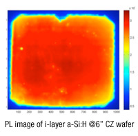
Examples for layers on wafer placed on hole carrier plates:
Multiple layers (layer stacks) may be deposited in one reactor without any interruption of the vacuum.
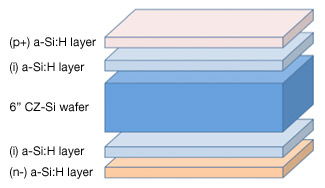
Example:
PECVD deposition of intrinsic and doped a-Si:H layers onto Si wafers for the manufacture of hetero-junction PV cells.