Our Technology - PVD

PVD module

W

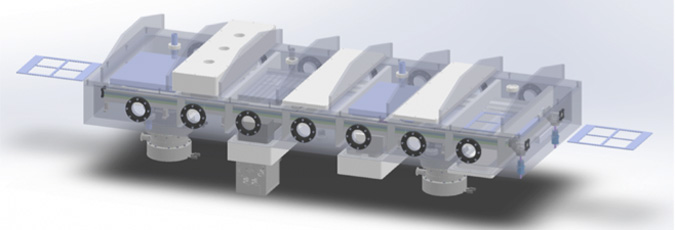
ith the OCTOPUS II system generation an inline PVD deposition module is available, which facilitates complete deposition cycles of substrates or wafers (for example, heterojunction devices) in one tool, without additional handling and vacuum breakage.

The module has been designed for top and bottom side deposition in one single run.

PVD
PVD Layers

Typical applications

  • Transparent conductive layers (TCO), such as ITO,
    ZnO, ZnO:Al etc
  • Metallization layers for back contacting (Ag, Mo,
    Al etc.)
     

Technical features

  • DC, pulsed DC or RF sputtering modes available
  • Planar or rotary cathode positions
  • Separate loading/unloading port